- 您现在的位置:买卖IC网 > Sheet目录1998 > ICS843251AGI-14LF (IDT, Integrated Device Technology Inc)IC CLK GEN ETHERNET 25MHZ 8TSSOP
ICS844251-14
FEMTOCLOCK CRYSTAL-TO-LVDS CLOCK GENERATOR
IDT / ICS LVDS CLOCK GENERATOR
3
ICS844251BG-14 REV. A NOVEMBER 19, 2012
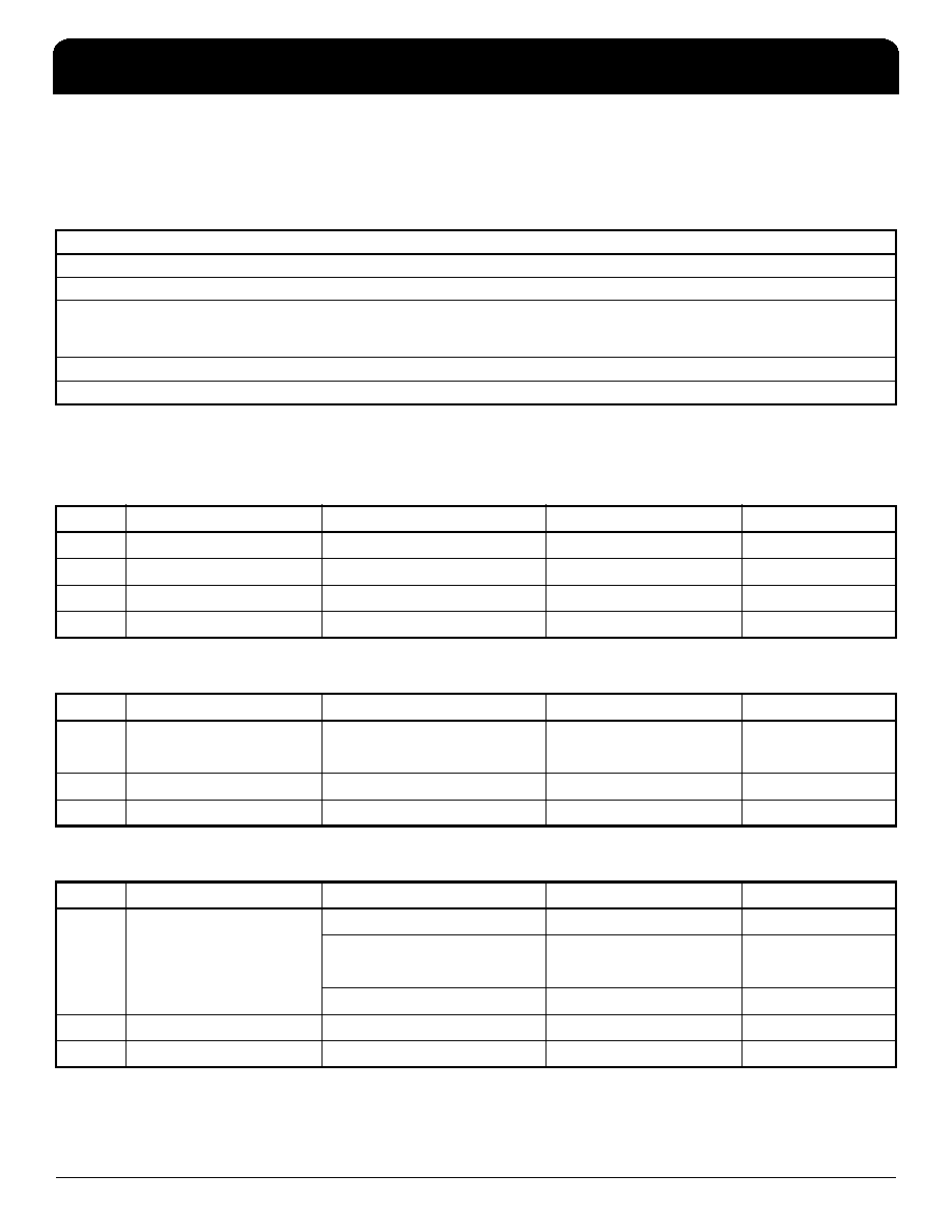
Absolute Maximum Ratings
NOTE: Stresses beyond those listed under Absolute Maximum Ratings may cause permanent damage to the device.
These ratings are stress specifications only. Functional operation of product at these conditions or any conditions beyond
those listed in the DC Characteristics or AC Characteristics is not implied. Exposure to absolute maximum rating conditions for
extended periods may affect product reliability.
DC Electrical Characteristics
Table 3A. Power Supply DC Characteristics, VDD = 3.3V ± 5%, TA = 0°C to 70°C
Table 3B. Power Supply DC Characteristics, VDD = 2.5V ± 5%, TA = 0°C to 70°C
Table 3C. LVCMOS/LVTTL DC Characteristics, VDD = 3.3V ± 5% or 2.5V ± 5%, TA = 0°C to 70°C
Item
Rating
Supply Voltage, VDD
4.6V
Inputs, VI
-0.5V to VDD + 0.5V
Outputs, IO
Continuos Current
Surge Current
10mA
15mA
Package Thermal Impedance,
JA
129.5
C/W (0 mps)
Storage Temperature, TSTG
-65
C to 150C
Symbol
Parameter
Test Conditions
Minimum
Typical
Maximum
Units
VDD
Core Supply Voltage
3.135
3.3
3.465
V
VDDA
Analog Supply Voltage
VDD – 0.10
3.3
VDD
V
IDD
Power Supply Current
100
mA
IDDA
Analog Supply Current
10
mA
Symbol
Parameter
Test Conditions
Minimum
Typical
Maximum
Units
VDD
Core Supply Voltage
2.375
2.5
2.625
V
VDDA
Analog Supply Voltage
VDD – 0.10
2.5
VDD
V
IDD
Power Supply Current
95
mA
IDDA
Analog Supply Current
10
mA
Symbol
Parameter
Test Conditions
Minimum
Typical
Maximum
Units
VIH
Input High Voltage
VDD = 3.465V
2
VDD + 0.3
V
VDD = 2.625V
1.7
VDD + 0.3
V
VIL
Input Low Voltage
VDD = 3.465V
-0.3
0.8
V
VDD = 2.625V
-0.3
0.7
V
IIH
Input High Current
VDD = VIN = 3.465V or 2.625V
150
A
IIL
Input Low Current
VDD = 3.465V or 2.625V, VIN = 0V
-5
A
发布紧急采购,3分钟左右您将得到回复。
相关PDF资料
ICS843251BGI-12LF
IC CLK GENERATOR LVPECL 8-TSSOP
ICS843251BGI-15LF
IC CLK GEN ETHERNET 25MHZ 8TSSOP
ICS843253AGI-45LF
IC SYNTHESIZER LVPECL 16-TSSOP
ICS8432DY-101LFT
IC SYNTHESIZER 700MHZ 32-LQFP
ICS8432DYI-101LF
IC SYNTHESIZER 700MHZ 32-LQFP
ICS843SDNAGLF
IC GENERATOR FEMTOCLOCK 8TSSOP
ICS844001AGLFT
IC CLK GEN FIBRE CHAN 8-TSSOP
ICS844002AG-01LF
IC SYNTHESIZER 2LVDS 20-TSSOP
相关代理商/技术参数
ICS843251AGI-14LFT
功能描述:IC CLK GEN ETHERNET 25MHZ 8TSSOP RoHS:是 类别:集成电路 (IC) >> 时钟/计时 - 时钟发生器,PLL,频率合成器 系列:HiPerClockS™, FemtoClock™ 标准包装:1,000 系列:- 类型:时钟/频率合成器,扇出分配 PLL:- 输入:- 输出:- 电路数:- 比率 - 输入:输出:- 差分 - 输入:输出:- 频率 - 最大:- 除法器/乘法器:- 电源电压:- 工作温度:- 安装类型:表面贴装 封装/外壳:56-VFQFN 裸露焊盘 供应商设备封装:56-VFQFP-EP(8x8) 包装:带卷 (TR) 其它名称:844S012AKI-01LFT
ICS843251BGI-12
制造商:ICS 制造商全称:ICS 功能描述:FEMTOCLOCKS⑩ CRYSTAL-TO-3.3V, 2.5V LVPECL CLOCK GENERATOR
ICS843251BGI-12FT
制造商:ICS 制造商全称:ICS 功能描述:FEMTOCLOCKS⑩ CRYSTAL-TO-3.3V, 2.5V LVPECL CLOCK GENERATOR
ICS843251BGI-12LF
功能描述:IC CLK GENERATOR LVPECL 8-TSSOP RoHS:是 类别:集成电路 (IC) >> 时钟/计时 - 时钟发生器,PLL,频率合成器 系列:HiPerClockS™, FemtoClock™ 标准包装:27 系列:Precision Edge® 类型:频率合成器 PLL:是 输入:PECL,晶体 输出:PECL 电路数:1 比率 - 输入:输出:1:1 差分 - 输入:输出:无/是 频率 - 最大:800MHz 除法器/乘法器:是/无 电源电压:3.135 V ~ 5.25 V 工作温度:0°C ~ 85°C 安装类型:表面贴装 封装/外壳:28-SOIC(0.295",7.50mm 宽) 供应商设备封装:28-SOIC 包装:管件
ICS843251BGI-12LFT
功能描述:IC CLK GENERATOR LVPECL 8-TSSOP RoHS:是 类别:集成电路 (IC) >> 时钟/计时 - 时钟发生器,PLL,频率合成器 系列:HiPerClockS™, FemtoClock™ 标准包装:1,000 系列:- 类型:时钟/频率合成器,扇出分配 PLL:- 输入:- 输出:- 电路数:- 比率 - 输入:输出:- 差分 - 输入:输出:- 频率 - 最大:- 除法器/乘法器:- 电源电压:- 工作温度:- 安装类型:表面贴装 封装/外壳:56-VFQFN 裸露焊盘 供应商设备封装:56-VFQFP-EP(8x8) 包装:带卷 (TR) 其它名称:844S012AKI-01LFT
ICS843251BGI-12T
制造商:ICS 制造商全称:ICS 功能描述:FEMTOCLOCKS⑩ CRYSTAL-TO-3.3V, 2.5V LVPECL CLOCK GENERATOR
ICS843251BGI-15
制造商:Integrated Device Technology Inc 功能描述:IC SYNTHESIZER LVPECL 8TSSOP
ICS843251BGI-15LF
功能描述:IC CLK GEN ETHERNET 25MHZ 8TSSOP RoHS:是 类别:集成电路 (IC) >> 时钟/计时 - 时钟发生器,PLL,频率合成器 系列:HiPerClockS™, FemtoClock™ 标准包装:27 系列:Precision Edge® 类型:频率合成器 PLL:是 输入:PECL,晶体 输出:PECL 电路数:1 比率 - 输入:输出:1:1 差分 - 输入:输出:无/是 频率 - 最大:800MHz 除法器/乘法器:是/无 电源电压:3.135 V ~ 5.25 V 工作温度:0°C ~ 85°C 安装类型:表面贴装 封装/外壳:28-SOIC(0.295",7.50mm 宽) 供应商设备封装:28-SOIC 包装:管件